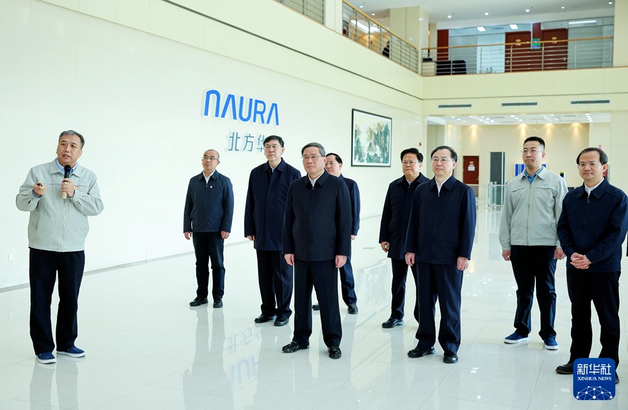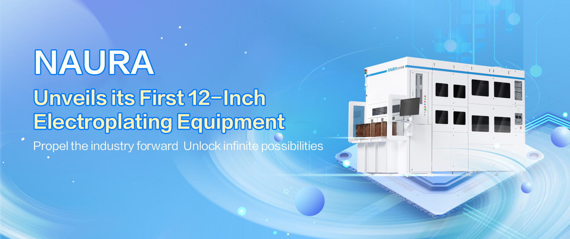


NAURA Unveils its First 12-Inch Electroplating Equipment


Recently, NAURA has formally released its first 12-inch electroplating equipment (ECP)—Ausip T830. It is designed for copper filling of through silicon vias (TSVs), mainly for use in the field of 2.5D/3D advanced packaging. It marks NAURA's official move into the electroplating equipment market, and a complete interconnection solution including etching, stripping, PVD, CVD, electroplating, PIQ and cleaning equipment has been established for the advanced packaging field.

Electroplating serves as the back-end process of physical vapor deposition (PVD), and the electroplating equipment cooperates with the PVD equipment for extensive application in the chip manufacturing processes such as logic, storage, power devices, and advanced packaging. In the process flow, the PVD equipment firstly forms a seed crystal layer in a slot/hole, and the electroplating equipment then fully fills the slot/hole till no voids. With the rapid development of advanced packaging and three-dimensional integration technologies, the global market size of the electroplating equipment has reached RMB8–9 billion each year, and is still escalating at high speed, which is expected to exceed 10 billion in the next few years.
NAURA's Ausip T830 is based on more than 30 key breakthrough technologies, exhibiting deep technical strength. It can optimize pre-wetting and electroplating parameters in real time using high vacuum sealing and electrochemical deposition technologies, to achieve the TSV filling at high aspect ratio. The electric field, flow field and chemical concentration are optimized to allow for uniform copper deposition inside and on the edge of TSV, which reduces defects and improves the yield and reliability of chips. It has a bilayer twin-chamber architecture to handle with two wafers at the same time, thereby improving the production capacity and saving the space. The customized air cylinder and sealing structure enhances the stability and reduces the maintenance cost. The intelligent liquid supplement system reduces the usage of additives, contributing to green manufacturing. Ausip T830 allows for modular customization and subsequent technological upgrades to meet diverse requirements. At present, it offers the uniform electroplated coating that meets customer requirements and can effectively fill a variety of perforated products with the hold diameter of 2–12 microns and the hole depth of 16–120 microns.

Looking ahead, NAURA will seize the opportunities for the development of advanced packaging and continuously increase the investment in research and development, striving to create a complete solution for the field of advanced packaging. Also, NAURA will continue to keep deep cooperation with customers to jointly promote the development of advanced packaging technology, boosting the chip industry to step on a new horizon.